It should come as no surprise that our data-driven business culture is significantly influencing the design and construction of semiconductor manufacturing facilities, or 'fabs', as they are known in the semiconductor industry.
As the coin of the realm in most aspects of business, semiconductor data has ushered in real progress in the semiconductor industry. As the coin of the realm in most aspects of business, semiconductor data has ushered in real progress in the semiconductor industry. Together with 3D modeling, it has enabled the development of accurate and data-rich engineering and construction digital twins in manufacturing. In turn, these enabled workflows such as offsite manufacturing (OSM) and modularization to speed up fabrication, assembly, and installation, to improve on-site safety and reduce the overall expense and duration of construction for the fabs.
Digital twins: streamlining semiconductor fab design and construction
Over the past five years or so, digital twins in manufacturing (the crossroads of 3D mapping, data, analytics, and systems) have paved the way for offsite manufacturing and prefabrication, leading to better, faster, and more efficient design of semiconductor facilities. This technological advancement spans the entire facility lifecycle, from design and engineering, to construction, equipment installation, and operations—all the way to redesign or renovation, re-tooling, demolition or recycling, to end of life.
Data-rich digital twins in manufacturing are still a relatively new concept in the context of semiconductor manufacturing design and construction. As a result, the data component is sometimes given short shrift in the project management process. Organizing a wide-reaching project like this requires sufficient upfront planning to fully understand the role of semiconductor data from the very beginning.
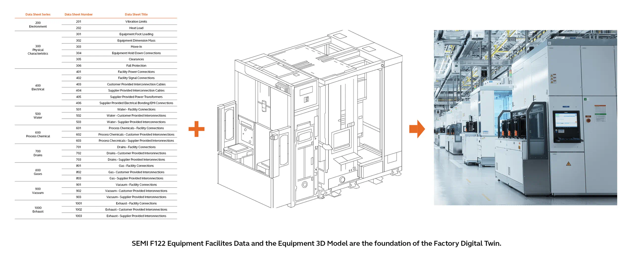
Digital twins in manufacturing are the culmination of numerous data-driven technologies. Laser scanning and 3D reality capture, for example, have greatly improved existing 2D and 3D documentation, enabling virtual design and construction workflows. The illustration below shows how semiconductor data drives the digital twin concept from beginning to end, to yield a “smarter” overall semiconductor manufacturing process.
The right time for data
From my experience with numerous fab projects over the years, I can say that too often, there is a rush to get started on a project. This rush can come at the expense of gathering required semiconductor data and information upfront, and effectively deploying it into the applicable data-related technologies.
So, at the risk of belaboring the subject, here are some pieces of advice that will help make your next project a success.
Data has upfront value
Data and information are currency. They have value. What some may not fully grasp, however, is that the value of semiconductor data can actually be realized at the front end of the project.
Designers and other project stakeholders need to take all the time required to gather information from the client, and to check, validate, and refine the data at the outset of the project. The more high-quality, accurate semiconductor data and information you can get at the start, the greater the payback will be throughout the entire semiconductor manufacturing life cycle.
These two standards come together first to design and construct the facility, then to install the manufacturing equipment, and then further feed into the fab operations and manufacturing. Therefore, integrating these standards before the project begins is fundamental to its success, and it is made easier because of the high-quality data you have gathered along the way.
Data and information, and the technologies utilizing it, are dramatically evolving semiconductor fab design and construction landscape. By taking the steps outlined here, we can make the most of all available technologies, and enable better project outcomes for fab owners and suppliers.
